
New Delhi, Jun 29: Researchers have built a computer from scratch without silicon, a “milestone” in showing that it is possible to one day replace the material that fuelled the bulk of technology advancements over the past half a century, by making devices smaller and faster.
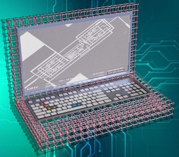
Built at a nanofabrication unit at The Pennsylvania State University in the US, the research team has demonstrated the successful working of the world’s first CMOS computer made using two-dimensional materials, which are paper-thin, but at the nano-level. It is described in a paper in the journal Nature.
‘Complementary Metal-Oxide-Semiconductor’, or CMOS, is widely used in designing electronic circuits. It consumes low power and accommodates more components.
The development is acknowledged as pioneering and a starting point in creating not just alternatives to silicon, but a roadmap for a new generation of still smaller, more flexible electronics.
Saptarshi Das, professor of engineering science and mechanics at the The Pennsylvania State University (Penn State), and lead researcher on the paper, told PTI, “In the short term, you would like to augment silicon with these two-dimensional (2D) materials, because they offer new functionalities — including in sensors and memory devices.
“This is why our paper is, I would say, a milestone, because it shows that it is possible in a way to replace silicon one day,” Das said.
Silicon, whose conductivity can be manipulated for controlling electricity flow, has been foundational in advancing technology by helping electronics shrink in size, since 1947 when a transistor was first made using the material.
A transistor regulates electric signals and acts as a building block for an electronic circuit.
But now, nearly seven decades later, as electronic devices continue to become smaller, silicon may have hit a wall — scientists say it may not be able to function as well, if devices are to get tinier.
Das said, “The trajectory of silicon has stalled.” Lead author Subir Ghosh, a doctoral student at Penn State, explains, “We have used molybdenum disulphide (MoS2) and tungsten diselenide (WSe2) — both quite common in the 2D materials community — to make our semiconductor devices.” “Here at Penn State, you can grow this material over a large two-inch wafer. They are also scaleable, which means that the industry can also adopt these 2D material,” Ghosh added.
The semiconductor industry is said to be governed by Moore’s law, according to which the number of transistors in circulation double every 18 months (a year and a half).
However, transistors are no longer becoming smaller. This is because silicon is a bulky material — like a brick — which cannot be made any smaller owing to detrimental effects, such as an increased leakage current, power consumption and a reduced performance of the device, Das explained over a video call.
“Now, for example, if we need to construct a multi-storied building, we will use bricks. But now, what if I tell you that the best choice for this building is not bricks — but paper, which is extremely thin. You can then get back all the good qualities you need to make a device very small,” Das said.
Research teams around the world, including China, are fiercely working for over a decade in developing 2D materials to initially support silicon in making smaller devices, but eventually transition away from having to use the bulky material itself.
Scientists at China’s Fudan University have created a RISC-V microprocessor chip by assembling transistors made of 2D materials. The chip, described in a paper published in April in the journal Nature, also used a low power to function.
Mayank Shrivastava, professor at the division of electrical, electronics and computer sciences, Indian Institute of Science, Bengaluru, and not involved in the study, told PTI, that a successful demonstration of the computer built using 2D materials is pioneering and “marks a watershed moment in the evolution of semiconductor technology.” “While we have seen individual devices and simple circuits from 2D materials before, building an actual computer, even one with a single instruction set, completely from 2D semiconductors is a bold leap,” he said.
Shrivastava added that these developments are also a “wake-up call that the silicon race is maturing, and the next race, based on 2D materials, has already begun”.
Das from Penn State explained that the 2D computer — a primitive one that present day semiconductor foundries might be building in the 1960s — was designed to perform a single instruction, which on repeat, can do all the basic functions of addition, subtraction and multiplication.
Ghosh explained this single instruction, named ‘reverse subtract, skip if borrow’.
“In order to subtract, you have two numbers. But while subtracting a bigger number from a smaller one, we need to ‘borrow’. So, when a ‘borrow’ is raised, our computer will skip that instruction and move on to the next,” the lead author said.
The computer achieved a high drive current, with a low leakage and power dissipation, enabling 2D-semiconductor circuits to operate below three volts and up to 25 kiloHertz of frequency, the study says.
Shrivastava, not involved in the study, said 2D materials hold the promise of pushing electronics beyond what silicon alone can offer.
“With atomic-scale thickness, high mobility, and near-ideal electrostatic control, these materials are natural candidates for continuing Moore’s Law in spirit, through performance-per-watt improvements, ultra-low leakage, and unprecedented device scaling,” he said.
The field of 2D materials — no longer a ‘potential’ one, but a strategic imperative — offers a rare opportunity to leapfrog into next-generation semiconductor leadership, he added.
However, the Penn State study’s limitations need to be considered, the IISc professor said.
“The operating speed of 25 kiloHertz is still far behind silicon, while challenges remain in improving channel mobility, gate oxides, contacts, managing parasitics, reliability, ensuring yield, and achieving top-gate device integration or nanosheet devices for scale,” he said.
“It is also vital to emphasise that while this milestone is academically significant, its commercial translation hinges on building infrastructure — testbeds, fabrication capabilities, tool ecosystems, and skillsets — that don’t yet exist in many countries.” Despite the limits, Shrivastava described the 2D computer as a “foundational milestone that, over time, have historically driven transformative changes.” On Friday, India’s electronics and IT Ministry was reported to consider funding research on 2D materials.
They plan on floating expressions of interest for selecting which projects to fund, officials said. (Agencies)


